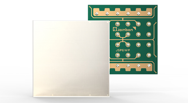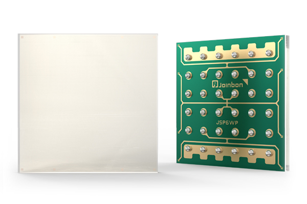
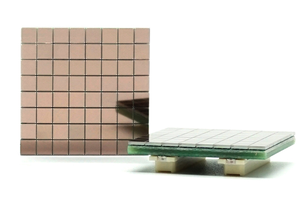


On June 19th, Joinbon Technology released the new TP series SiPM. The TP series SiPM is manufactured on CMOS process and uses a new wafer-level package based on TSV technology to effectively reduce device size and dead space, great improvement in uniformity and reliability.
Compared with the TN series SiPM, the TP series achieves a package area of 9.3636mm2 under the same 9mm2 sensor chip area, which is 41.5% smaller than the TN series. The dead zone outside the photosensitive area is almost completely eliminated, and the structure is more compact, making the TP series is very suitable for large area array detection. Compared with the TN series Array, the overall detection efficiency of the array can be increased by more than 30%, which greatly enhances the photon signal capture capability under large area array.

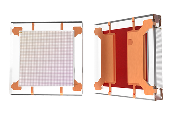
Structural optimization and improved package accuracy provide better uniformity for the TP Series SiPM. The traditional package uses the wire bonding method to connect the chip electrode and the lead frame. The length of the wire is different and the size of the lead frame fluctuates, so that the fluctuation of the signal path reaches the millimeter level. But the wafer level package is vertical connection through the through silicon via (TSV). High-precision lithography routing, signal path length fluctuations reduced to micron level, smaller path fluctuations can effectively reduce signal transmission jitter, thus achieving better uniformity of the TP series.
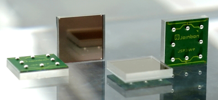
In addition, the new TP series SiPM products use high-strength special glass as the cover material, which has higher reliability, better temperature stability and longer life than silicone grease.
The wafer-level package based on TSV technology also known as wafer level chip scale package (WL-CSP), which is an advanced packaging method that completes the packaging process directly at the wafer level. TSV-based wafer-level packaging uses silicon via + lithography to achieve chip I\O interconnection, resulting in package size = chip size, greatly improving device package compactness and reliability, making the device light thin, small, reliable, efficient, accurate, etc. which is the key development direction of SiPM packaging.
At present, the following models of TP series SiPM have begun to accept orders, the specific parameters are as follows, welcome to consult.
|
Parameter |
Value |
Condition |
Unit |
|
|
JSP-TP3050-SMT |
||||
|
Spectral Response Range |
250-950 |
-- |
nm |
|
|
Peak Sensitivity Wavelength |
420 |
-- |
nm |
|
|
PDE |
35% |
Vov=2V |
-- |
|
|
Gain |
2.5×10⁶ |
Vov=2V |
-- |
|
|
Rise Time |
1 |
Vov=2V |
ns |
|
|
Dark Count Rate |
Type |
120 |
Vov=2V |
kHz/mm2 |
|
Max |
270 |
Vov=2V |
||
|
Temperature Dependency of Vbr |
34.4 |
-- |
mV/℃ |
|
|
Crosstalk Probability |
3.1% |
Vov=2V |
-- |
|
|
Afterpulse |
3.9% |
Vov=2V |
-- |
|